






Elif Özaksu
Corporate
- Thread Author
- #1
💡 Why Advanced Packaging?
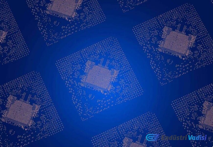
The increasing demand for processing power in areas such as artificial intelligence, high-performance computing, and industrial devices is pushing the limits of traditional single-chip architectures. To overcome these limitations and shorten data transmission paths, the semiconductor industry is turning to advanced packaging architectures, supported by TRUMPF's specialized laser, plasma, and process metrology technologies.
🧠 Multi-Chip Integration: The Key to Performance
Advanced packaging addresses performance constraints by combining multiple specialized chips with different functions, such as computation and memory, into a single system. These chips can be placed side-by-side or stacked vertically in three dimensions. Ultra-fine electrical connections shorten signal distances, increasing bandwidth and energy efficiency, while the package structure must reliably dissipate intense thermal loads.
🔬 Manufacturing Challenges and TRUMPF Solutions
The mass production of modern chip packages, involving millions of microscopic structures, thin material layers, and delicate surfaces, presents significant engineering challenges. TRUMPF brings together three core industrial competencies to make these complex process steps industrially controllable: plasma generation, precise laser micro-machining, and metrology.
⚡ Plasma Generation: Precise Etching and Interconnect Metallization
Plasma is a fundamental element in semiconductor manufacturing for creating and selectively removing thin material layers. In advanced packaging workflows, plasma processes are used to create fine interconnect structures and contact surfaces that route electrical signals between stacked or adjacent chips. TRUMPF's plasma generators precisely control these etching and deposition processes, ensuring uniform micro-structuring, controlled layer formation, and reliable electrical connections.
✨ Superior Lasers: Glass Vias and Chip Singulation
Advanced packaging pushes mechanical processing to its physical limits with delicate new materials such as thin wafers, dense substrates, glass interposers, and thin redistribution layers. TRUMPF's ultra-short pulse lasers process these materials contact-free, performing cutting, drilling, structuring, marking, localized heating, ablation, and bonding with high precision. In particular, they play a critical role in drilling vias, which are microscopic vertical connection holes that electrically connect different levels within the chip package. Laser systems are also used for structuring fine conductive paths and for the clean singulation of individual chips and packages.
💎 Glass Substrates and Next-Generation Thermal Materials
To increase package density and manufacturing economics, semiconductor manufacturers are evaluating glass as an alternative to silicon for interposers. Glass offers favorable thermal properties, high surface flatness, and the ability to be processed in rectangular panel formats instead of round wafers, reducing material waste and increasing unit yield. Precise laser processing is indispensable for drilling fine, crack-free holes in brittle glass at production speeds.
For high-power packages, thermal management drives parallel material research. Silicon carbide is gaining attention for integrated microfluidic cooling channels because it combines high thermal conductivity with thermal expansion properties compatible with silicon. In the longer term, synthetic diamond is being investigated as a high-performance substrate material.
📊 Inline Metrology: For High-Volume Series Production
As interconnect pitches shrink and the complexity of vertical chip stacking increases, continuous process monitoring becomes indispensable. Measuring and inspecting every manufacturing step, known as metrology, allows engineers to detect deviations in layer thicknesses, surface topography, drilled via geometries, contact points, and inter-layer alignment early on. In addition to plasma and laser hardware, TRUMPF also provides the process control expertise and high-power laser tools needed to keep highly integrated chip architectures stable over millions of production cycles.
🔍 Transition to Glass Core Substrates
The transition from organic laminate substrates and silicon interposers to glass core substrates represents a significant structural shift in 2.5D and 3D semiconductor packaging. While traditional organic substrates experience warpage under thermal cycling and exhibit higher dielectric losses at multi-gigahertz frequencies, silicon interposers remain limited by circular wafer sizes and higher material costs. Glass provides superior dimensional stability and inherent electrical insulation, reducing parasitic capacitance through Through-Glass Vias (TGVs).
Unlike organic printed circuit boards, which tolerate mechanical drilling or standard carbon dioxide laser ablation, glass exhibits brittle fracture behavior with almost no plastic deformation. Mechanical contact or thermal ablation causes residual stress and micro-cracks that can propagate across an entire panel. Therefore, industry standards for TGV formation typically rely on contact-free ultra-short pulse lasers operating in the picosecond or femtosecond regime, often paired with selective wet chemical etching, to achieve crack-free, high aspect ratio vias with controlled taper angles. Subsequent metallization of these deep, narrow glass vias requires advanced plasma physical vapor deposition techniques, such as High Power Impulse Magnetron Sputtering (HiPIMS), which enhances metal ion density to ensure uniform conductive seed layer coverage without void formation along the vertical sidewalls.